DE Model Exam – Part C (10 Marks)
Q 29. Decimal ↔ Binary, Octal, Hexadecimal Conversion
🔹 Decimal to Binary:
- Divide the decimal number by 2 repeatedly.
- Write down remainders in reverse order.
Example:
(13)₁₀ = (1101)₂
(13 ÷ 2 = 6 R1, 6 ÷ 2 = 3 R0, 3 ÷ 2 = 1 R1, 1 ÷ 2 = 0 R1)
🔹 Binary to Decimal:
- Multiply each bit by 2ⁿ and add.
(1101)₂ = (1×8 + 1×4 + 0×2 + 1×1) = (13)₁₀
🔹 Decimal to Octal:
- Divide by 8 repeatedly.
(125)₁₀ = (175)₈
🔹 Octal to Decimal:
(175)₈ = (1×8² + 7×8¹ + 5×8⁰) = (125)₁₀
🔹 Decimal to Hexadecimal:
- Divide by 16, take remainders (A–F for 10–15).
(254)₁₀ = (FE)₁₆
🔹 Hexadecimal to Decimal:
(FE)₁₆ = (15×16 + 14×1) = 254
👉 Importance:
Used in Microprocessor, Memory address representation, and Digital Circuit Design.
Q 30. Operation of Logic Gates – AND, OR, NOT, NAND, XNOR
Logic Gates are basic building blocks of digital circuits.
They perform logical operations using binary inputs (0 / 1).
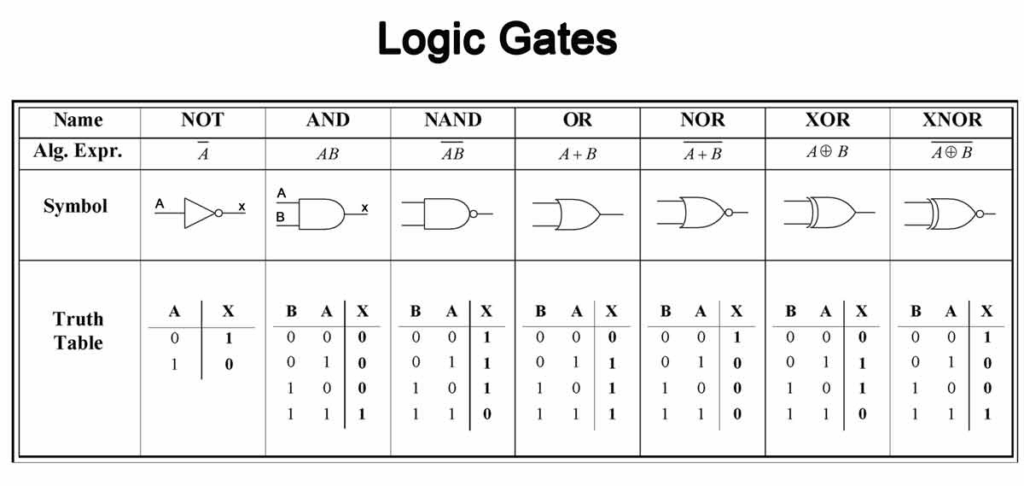
👉 Note: NAND and NOR are Universal Gates – any circuit can be made using them alone.
Q 31. Full Adder – Operation with Diagram
Definition:
A Full Adder adds three binary bits (A, B and Cₙ₋₁ or Carry in) and produces Sum and Carry out.
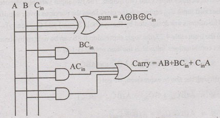
🔹 Logic Diagram:
(Use two Half Adders + OR gate)
🔹 Truth Table:
| A | B | Cin | Sum | Cout |
|---|---|---|---|---|
| 0 | 0 | 0 | 0 | 0 |
| 0 | 0 | 1 | 1 | 0 |
| 0 | 1 | 0 | 1 | 0 |
| 0 | 1 | 1 | 0 | 1 |
| 1 | 0 | 0 | 1 | 0 |
| 1 | 0 | 1 | 0 | 1 |
| 1 | 1 | 0 | 0 | 1 |
| 1 | 1 | 1 | 1 | 1 |
🔹 Boolean Expressions:
Sum = A ⊕ B ⊕ Cin
Carry = AB + BCin + ACin
👉 Use:
Binary addition in ALU, microprocessors, digital counters.
Q 32. JK Flip-Flop – Working with Diagram and Truth Table
Definition:
A JK Flip-Flop is a bistable sequential circuit having two inputs (J and K) and one clock signal.
It can set, reset and toggle its output.
🔹 Symbol & Block Diagram:
Inputs – J, K, Clock → Outputs – Q, Q′
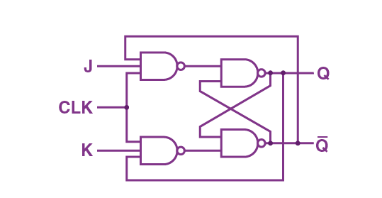
🔹 Truth Table:
| J | K | Q(next) | Operation |
|---|---|---|---|
| 0 | 0 | No change | Memory |
| 0 | 1 | 0 | Reset |
| 1 | 0 | 1 | Set |
| 1 | 1 | Q′ | Toggle |
🔹 Excitation Table:
Used for designing sequential circuits.
🔹 Logic Diagram:
Combination of SR Latch + Feedback paths using AND gates controlled by Clock.
👉 Applications:
Used in Counters, Registers, Memory storage, Frequency division.
Q 33. Types of ROM – Explanation with Diagrams
ROM (Read Only Memory) stores data permanently even when power is off.
🔹 Types of ROM:
1️⃣ Mask ROM:
- Data programmed by manufacturer.
- Used for permanent firmware.
2️⃣ PROM (Programmable ROM):
- User can program once using PROM programmer.
- Cannot be erased.
3️⃣ EPROM (Erasable PROM):
- Can be erased by UV light (through quartz window).
- Reusable.
4️⃣ EEPROM (Electrically Erasable PROM):
- Can be erased and reprogrammed electrically.
- Used in microcontrollers, BIOS.
5️⃣ Flash ROM:
- Modern type of EEPROM, fast erasing in blocks.
- Used in USB drives, mobile memory.
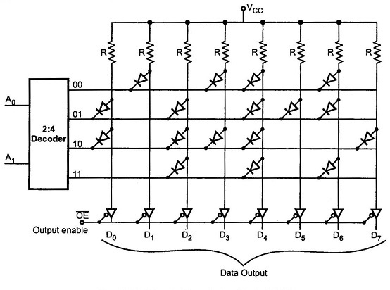
👉 Diagram:
Shows address decoder and memory cell array (rows × columns).
👉 Advantages:
- Non-volatile
- Reliable storage
- Low power consumption
👉 Applications:
Firmware storage, Embedded systems, BIOS, Microcontrollers.