Unit 2 Part – C
Q1. Input & Output Characteristics of CE Configuration
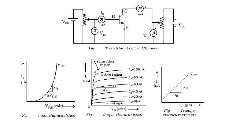
1️⃣ Input Characteristic (IB vs VBE):
- Resembles forward-biased diode curve.
- Base current increases exponentially with VBE.
2️⃣ Output Characteristic (IC vs VCE):
- Shows three regions:
- Cut-off Region → No IC, both junctions reverse-biased.
- Active Region → IC ∝ IB (used for amplification).
- Saturation Region → IC maximum, transistor fully ON.
3️⃣ Uses:
- To determine Q-point and transistor operation region.
Q2. Fixed Bias, Collector-to-Base Bias & Voltage Divider Bias
1️⃣ Fixed Bias:
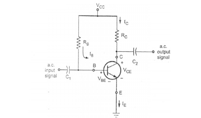
- Resistor Rb from base to Vcc.
- Simple, but poor thermal stability.
2️⃣ Collector-to-Base Bias:
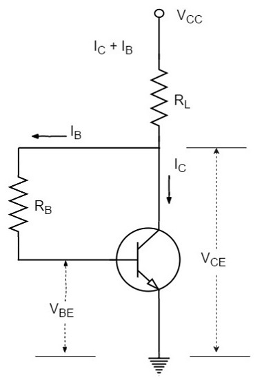
- Rb connected from collector to base.
- Provides negative feedback → improved stability.
3️⃣ Voltage Divider Bias:
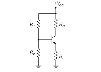
- Two resistors (R1, R2) form divider to set base voltage.
- Emitter resistor Re improves stability.
- Most widely used biasing method.
Comparison:
| Type | Stability | Components | Use |
|---|---|---|---|
| Fixed | Poor | Simple | Basic |
| Collector–Base | Moderate | 2 resistors | Improved |
| Voltage Divider | Best | 4 components | Industrial circuits |
Q3. Construction & Working of NPN Transistor
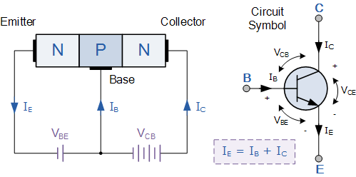
1️⃣ Construction:
- Two N-type separated by thin P-type base.
- Emitter: heavily doped, Base: thin & lightly doped, Collector: moderately doped.
2️⃣ Working:
- Emitter-base forward biased, collector-base reverse biased.
- Electrons from emitter → base → collector.
- Base current small, controls large collector current.
3️⃣ Application:
- Used as current amplifier, switch, and oscillator.
Q4. CE, CB, and CC Configurations
| Config | Input | Output | Current Gain | Voltage Gain | Phase |
|---|---|---|---|---|---|
| CE | Base–Emitter | Collector–Emitter | High | High | 180° shift |
| CB | Emitter–Base | Collector–Base | ≈ α (<1) | High | 0° |
| CC | Base–Collector | Emitter–Collector | >1 | ≈1 | 0° |
Use:
- CE: Amplifier
- CB: High frequency applications
- CC: Impedance matching
Unit 2 Part – C Tamil
Q1. Input & Output Characteristics of CE Configuration
Definition:
Common Emitter (CE) configuration-இல் transistor amplify பண்ணும் circuit arrangement.
Input = Base–Emitter, Output = Collector–Emitter terminals.
1️⃣ Input Characteristics (IB vs VBE):
- Forward bias apply பண்ணும்.
- Graph similar to diode forward characteristic.
- VBE ↑ → IB ↑ exponentially.
- Base current small, few microamperes range.
2️⃣ Output Characteristics (IC vs VCE):
- Reverse bias at collector junction.
- Curves for different IB values plot பண்ணப்படும்.
- Cut-off Region: IB = 0, transistor OFF.
- Active Region: IC ∝ IB → used for amplification.
- Saturation Region: IC maximum, transistor fully ON.
3️⃣ Use:
இந்த characteristic curves மூலம் transistor-இன் Q-point (operating point) fix பண்ணலாம்.
Q2. Fixed Bias, Collector-to-Base Bias, Voltage Divider Bias
1️⃣ Fixed Bias:
- Base resistor RB direct-ஆ VCC-க்கு connect பண்ணப்படும்.
- Simple circuit but poor stability.
- Temperature change-ஆனாலும் IC vary ஆகும்.
2️⃣ Collector-to-Base Bias:
- RB collector-இல் இருந்து base-க்கு connect பண்ணப்படும்.
- Negative feedback கிடைக்கும் → better stability.
- Thermal runaway reduce ஆகும்.
3️⃣ Voltage Divider Bias:
- Two resistors R1 & R2 voltage divider network.
- Emitter resistor RE stability improve பண்ணும்.
- Most stable bias method in amplifiers.
Comparison Table:
| Bias Type | Stability | Components | Use |
|---|---|---|---|
| Fixed | Poor | Simple | Basic circuits |
| Collector–Base | Moderate | 2 resistors | Feedback improve |
| Voltage Divider | Best | 4 components | Amplifiers |
Q3. Construction and Working of NPN Transistor
Construction:
- Two N-type materials separated by thin P-type base.
- Emitter: heavily doped → more electrons emit.
- Base: thin & lightly doped → few recombination.
- Collector: moderately doped → collects electrons.
Working Principle:
- Emitter–Base junction forward biased, Collector–Base reverse biased.
- Electrons from emitter enter base → few recombine → remaining reach collector.
- Small base current (IB) controls large collector current (IC).
- Hence transistor acts as current amplifier.
Applications:
- Used as amplifier, switch, oscillator circuits.
Q4. CE, CB, and CC Configurations
1️⃣ Common Emitter (CE):
- Input: Base–Emitter, Output: Collector–Emitter.
- High voltage & current gain, phase shift = 180°.
- Widely used amplifier configuration.
2️⃣ Common Base (CB):
- Input: Emitter–Base, Output: Collector–Base.
- Low input impedance, High output impedance.
- Current gain ≈ α (<1).
- Used for high frequency applications.
3️⃣ Common Collector (CC):
- Input: Base–Collector, Output: Emitter–Collector.
- Voltage gain ≈ 1, current gain high.
- Used for impedance matching (Buffer stage).
Summary Table:
| Type | Input | Output | Current Gain | Voltage Gain | Phase | Use |
|---|---|---|---|---|---|---|
| CE | Base–Emitter | Collector–Emitter | High | High | 180° | Amplifier |
| CB | Emitter–Base | Collector–Base | Low | High | 0° | HF circuits |
| CC | Base–Collector | Emitter–Collector | High | ≈1 | 0° | Buffer |